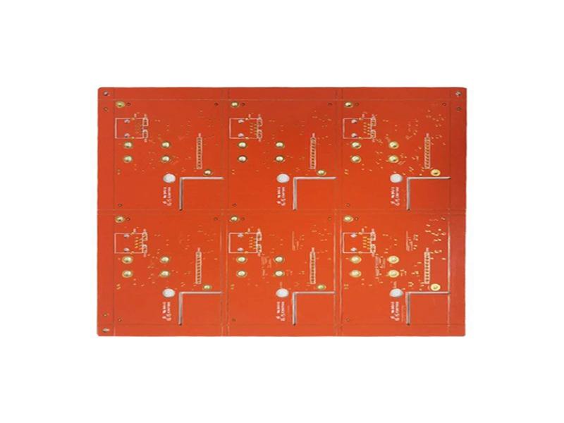
Red solder mask custom-make FR4 Rigid muilti-layer PCB
FR4 PCB Introduction
–Definition
FR means “flame-retardant,” FR-4 (or FR4) is a NEMA grade designation for glass-reinforced epoxy laminate material, a composite material composed of woven fiberglass cloth with an epoxy resin binder that makes it an ideal substrate for electronic components on a printed circuit board.
-Pros and Cons of FR4 PCB
- FR-4 material is so popular because of its many wondrous qualities that can benefit printed circuit boards. In addition to being affordable and easy to work with, it is an electrical insulator with very high dielectric strength. Plus, it’s durable, moisture-resistant, temperature-resistant and lightweight.
- FR-4 is a widely relevant material, popular mostly for its low cost and relative mechanical and electrical stability. While this material features extensive benefits and is available in a variety of thicknesses and sizes, it isn’t the best choice for every application, especially high-frequency applications like RF and microwave designs.
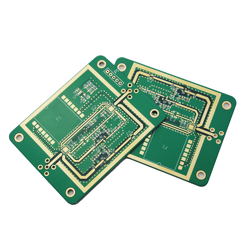
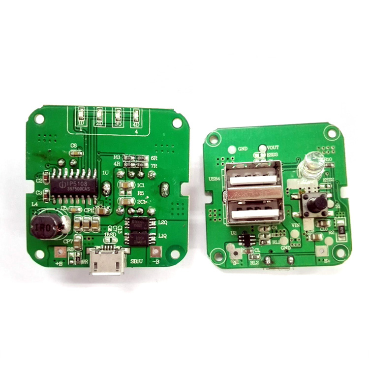
-Multi-layer PCB Structure
Multilayer PCBs further increases the complexity and density of PCB designs by adding additional layers beyond the top and bottom layers seen in double sided boards. Multilayer PCBs are built by laminating the various layers. The inner-layers, normally double-sided circuit boards, are stacked together, with insulating layers in between and between the copper-foil for the outer-layers. Holes drilled through the board (vias) will make connections with the different layers of the board.
Where does the resin material come from in ABIS?
Most of them from Shengyi Technology Co., Ltd. (SYTECH), who has been the world’s second largest CCL manufacturer in terms of sales volume, from 2013 to 2017. We established long-term relations of cooperation since 2006. The FR4 resin material (Model S1000-2, S1141, S1165, S1600) are mainly used for making single and double-sided printed circuit boards as well as multi-layer boards. Here comes details for your reference.
- For FR-4: Sheng Yi, King Board, Nan Ya, Polycard, ITEQ, ISOLA
- For CEM-1 & CEM 3: Sheng Yi, King Board
- For High Frequency : Sheng Yi
- For UV Cure: Tamura, Chang Xing ( * Available colour : Green) Solder for Single Side
- For Liquid Photo: Tao Yang, Resist (Wet Film)
- Chuan Yu ( * Available colours : White, Imaginable Solder Yellow, Purple, Red, Blue, Green, Black)
Rigid PCB Manufacturing Capacity
ABIS experienced in making special materials for rigid PCB, such as: CEM-1/CEM-3, PI, High Tg, Rogers, PTEF, Alu/Cu Base, etc. Below is a brief overview FYI.
| Item | Speci. |
| Layers | 1~20 |
| Board Thickness | 0.1mm-8.0mm |
| Material | FR-4, CEM-1/CEM-3, PI, High Tg, Rogers, PTEF, Alu/Cu Base, etc |
| Max Panel Size | 600mm×1200mm |
| Min Hole Size | 0.1mm |
| Min Line Width/Space | 3mil(0.075mm) |
| Board Outline Tolerance | 士0.10mm |
| Insulation Layer Thickness | 0.075mm–5.00mm |
| Out Layer Copper Thickness | 18um–350um |
| Drilling Hole (Mechanical) | 17um–175um |
| Finish Hole (Mechanical) | 0.10mm–6.30mm |
| Diameter Tolerance (Mechanical) | 0.05mm |
| Registration (Mechanical) | 0.075mm |
| Aspect Ratio | 16:1 |
| Solder Mask Type | LPI |
| SMT Mini. Solder Mask Width | 0.075mm |
| Mini. Solder Mask Clearance | 0.05mm |
| Plug Hole Diameter | 0.25mm–0.60mm |
| Impedance Control Tolerance | 士10% |
| Surface finish | ENIG, OSP, HASL, Chem. Tin/Sn, Flash Gold |
| Soldermask | Green/Yellow/Black/White/Red/Blue |
| Silkscreen | Red/Yellow/Black/White |
| Certificate | UL, ISO 9001, ISO14001, IATF16949 |
| Special Request | Blind hole, Gold finger, BGA, Carbon ink, peekable mask, VIP process, Edge plating, Half holes |
| Material Suppilers | Shengyi, ITEQ, Taiyo, etc. |
| Common Package | Vacuum+Carton |
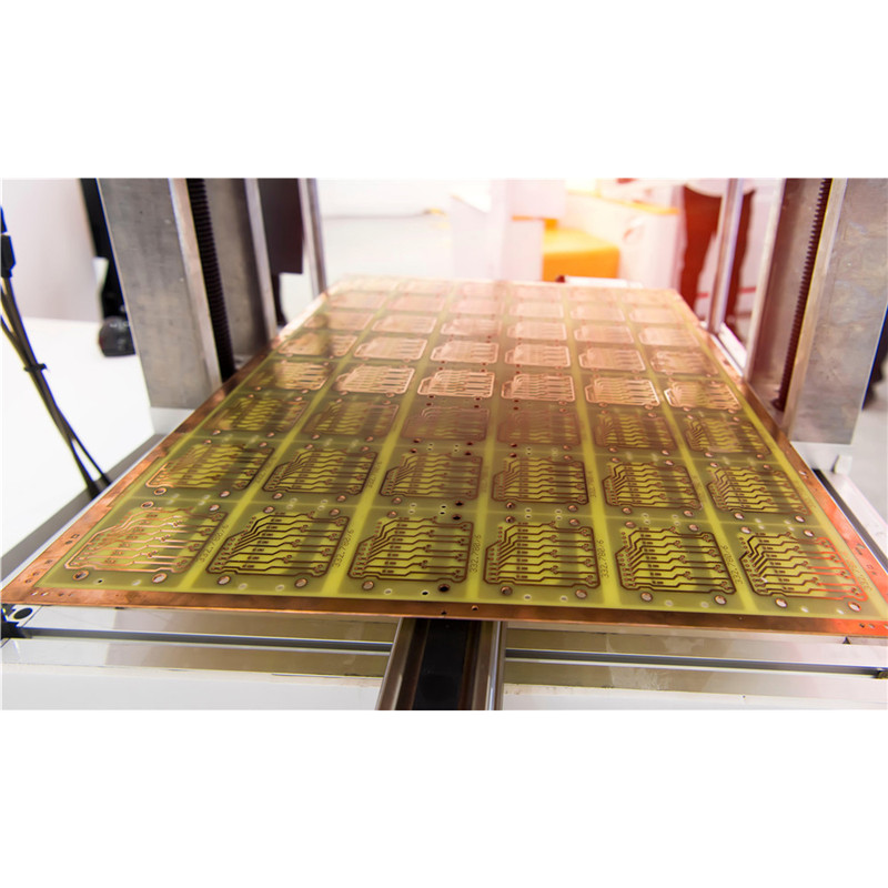
Multi-layer PCB Manufacturing Process
- The process starts with designing Layout of the PCB using any PCB designing software / CAD Tool (Proteus, Eagle, Or CAD).
- All rest of the steps are of Manufacturing Process of a Rigid Printed Circuit Board is same as Single Sided PCB or Double Sided PCB or Multi-layer PCB.