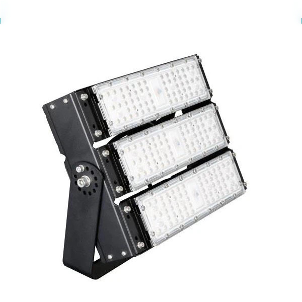
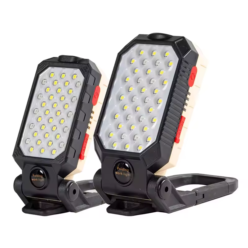
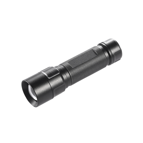
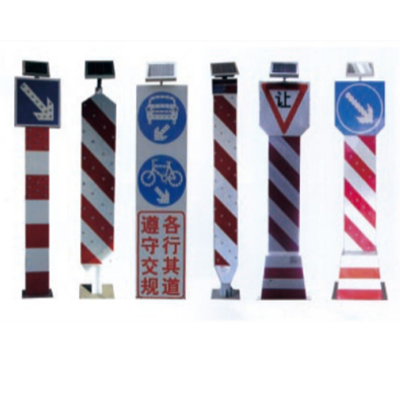
SMD LED Flood Lights
● Bridgelux 3030 chips;
● Meanwell ELG series driver
● 5 years Warranty
● Modular design, beautiful appearance.
Adopting die-casting aluminum alloy, this SMD LED flood light feature a robust body and lightweight, as well as good heat dissipation.
Our SMD LED flood lights use high efficiency SMD LED chips to produce high lumen output.
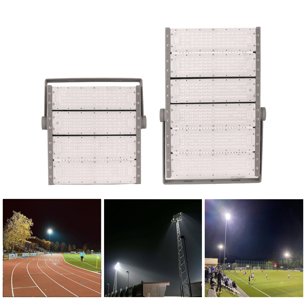
Suitable for different sports grounds, highways, driveways, pathways, parking lots, and other applications.
Technical data
| MN | Power (W) |
LED type/Qty | Efficiency |
Beam Angle |
Color |
Voltage & Frequency |
| -SMD-FL-50W | 50 | Bridgelux 3030/60pcs |
135lm/w or 170lm/w |
24, 36, 60,90, |
3000K/ 4000K /5000K |
AC 200-305V |
| -SMD-FL-100W | 100 | Bridgelux 3030/120pcs | ||||
| -SMD-FL-150W | 150 | Bridgelux 3030/180pcs | ||||
| -SMD-FL-200W | 200 | Bridgelux 3030/240pcs | ||||
| -SMD-FL-300W | 300 | Bridgelux 3030/360pcs | ||||
| -SMD-FL-400W | 400 | Bridgelux 3030/480pcs | ||||
| -SMD-FL-500W | 500 | Bridgelux 3030/600pcs | ||||
| -SMD-FL-600W | 600 | Bridgelux 3030/720pcs | ||||
| -SMD-FL-800W | 800 | Bridgelux 3030/960pcs | ||||
| -SMD-FL-1000W | 1000 | Bridgelux 3030/1200pcs |
Features
1. Super bright & energy saving
200W SMD LED flood lights include 4pcs light module, providing up to 27000lm high light output.
It is several times brightness higher than traditional light bulbs, which can save up to 80% electricity.
2. IP65 waterproof & different beam angle
With IP65 rating and unique optical concave-convex structure lens, this LED flood light can be widely used in outdoor and indoor lighting projects;
Different beam angles such as 150×70°, 140×100°, 24°, 36°, 60°, 90°are shadow-free and anti-glare, providing great bright light.
3. Durable material & excellent dissipation
The LED flood light outdoor are made of heavy duty die cast aluminum housing. The excellent heat dissipation can prolong LED lifespan to 50,000 hours.
4. Flexible Installation
The LED flood light comes with adjustable metal bracket and side bracket accessories, it can be installed in the ceiling, walls, ground and other locations, by adjusting the different angles.
5. After-sales service
We have a professional customer service team to provide support.
If you encounter any problems, please contact us. We always pursue 100% customer satisfaction; and provide quality services and satisfactory solutions.
Project References
Difference Between Smd Led Chips And Cob Led Chips
1. Packaging method:
1) SMD packaging through the SMD form of multiple discrete devices pasted on the PCB board to form the LED application light source components, such practices exist point light, glare and ghosting problems.
2) COB refers to Chip-On-Board, the low power chip directly packaged on the aluminum substrate for fast heat dissipation, small chip area, high heat dissipation efficiency, low drive current. Thus has a low thermal resistance, high thermal conductivity of high heat dissipation.
Compared with ordinary SMD small power light source features: higher brightness, small thermal resistance (<6℃/W), smaller light decay, higher apparent finger, perfect light spot, long life.
2. Production process :
1) The system thermal resistance of traditional SMD package application is: chip – solid crystal adhesive – solder joint – solder paste – copper foil – insulation layer – aluminum.
2) The system thermal resistance of COB package is: chip – solid crystal adhesive – aluminum.
COB package in the production process and the traditional SMD production process is basically the same, in the solid crystal, welding line process and SMD package efficiency is basically equivalent, but in the dispensing, separation, spectroscopy, packaging, COB package efficiency is much higher than SMD products.
Traditional SMD package labor and manufacturing costs account for roughly 15% of the cost of materials, COB package labor and manufacturing costs account for roughly 10% of the cost of materials, using COB package, labor and manufacturing costs can save 5%.
COB package system thermal resistance is much lower than that of traditional SMD package system thermal resistance, so it can significantly improve the lifetime of LED.
Write your message here and send it to us
